By the end of this lecture, students should be able to:
Explain the purposes of signal conditioning: amplification, level shifting, isolation, and filtering
State the Nyquist-Shannon sampling theorem and predict the aliased frequency of an undersampled tone
Explain why anti-aliasing filters must be analog and placed before the ADC, and design a first-order low-pass filter for that purpose
Choose a sampling rate for a given application, balancing bandwidth, storage, and aliasing concerns
Analyze basic operational amplifier configurations (inverting, non-inverting, differential/instrumentation amplifiers) under the ideal op-amp assumptions
NoteTopics Covered
Signal conditioning and its four jobs: amplification, level shifting, isolation, filtering
Conditioning blocks as LTI systems: impulse, magnitude, and phase response; Bode plots; where Laplace and z-transforms come in
Grounded and floating sources; differential, referenced, and non-referenced single-ended measurements; bias resistors
Sampling as multiplication by an impulse train; spectral replication
Aliasing and folding, revisited from the frequency domain
Anti-aliasing filters: why analog, why before the ADC, and first-order RC design
Ideal op-amp rules; inverting, non-inverting, difference, and instrumentation amplifiers
Choosing a sampling rate: bandwidth vs. storage vs. aliasing
6.1.1 Before You Begin
This lecture leans directly on Lecture 3 (RC circuits, impedance, Thévenin equivalents and loading) and Lecture 4 (the sampling theorem, the folding formula, quantization, and the ADC pipeline). The demos produce sound, so use headphones if you want to use them without disturbing anyone.
Every code block in this chapter assumes that the setup below has run first, in the same Python session: it imports the libraries and defines the names the blocks share (see About the code in the Welcome chapter).
The signals Lecture 2’s transducers actually produce — millivolt bridge imbalances, bipolar swings, waveforms that picked up noise on a long cable — are almost never exactly what Lecture 4’s ADC wants at its input pins. Signal conditioning is the circuit stage that closes this gap, and its four jobs — amplification, level shifting, isolation, and filtering — are all built from the LTI circuit blocks of Lecture 3 and sit strictly before the converter (the ADC itself is not conditioning).
Lecture 4 drew the acquisition pipeline as sensor → signal conditioning → multiplexer → sample-and-hold → ADC and then spent its time on the converter end. This section opens the box labeled “signal conditioning” (Figure 6.1). The unifying idea is one you already own: every block inside it is a linear time-invariant circuit, so each one is described by a gain, an offset, or a frequency response — and each exists because the converter has a fixed input range, a fixed reference, a single ground, and no opinion about which frequencies you meant to measure (Figliola and Beasley 2019).
Figure 6.1: Inside the signal-conditioning block of Lecture 4’s pipeline. Everything in the shaded box is analog and ends at the converter’s input pins; the order of the four jobs varies with the application, and not every channel needs all four.
TipActive Learning: Which jobs does each channel need?
Three channels, four jobs. For each, name the conditioning jobs it needs (possibly none, possibly all four) and why, using only what you know from Lectures 2–4:
a quarter-bridge strain gauge on a highway girder, read through 50 m of cable in a substation yard;
the GL5528 voltage divider from Assignment 1, on a desk, wired to the ESP32 next to it;
the ADXL335 accelerometer bolted to a pump housing, logged at 1 kS/s.
TipOne defensible answer
Amplify — millivolts must fill a volts-wide converter range; isolate — the girder and the logger may not share a ground, and a substation yard is the textbook place for stray potentials; filter — 50 m of cable is an antenna for 60 Hz hum. (2) Almost nothing: the divider already produces a volt-scale, ground-referenced, slowly varying signal; at most a low-pass against flicker (see Section 6.4). (3) Level-shift is done inside the part (it rests at mid-supply); the pump motor argues for a filter, and the 1 kS/s rate makes that filter an anti-aliasing filter with a cutoff to be designed, not guessed.
6.2.1 Conditioning Blocks as LTI Systems
Four jobs, four kinds of circuit — and yet every datasheet describes them with the same three or four numbers. That is no coincidence: an amplifier, a level shifter, an isolator, and a filter are all linear time-invariant (LTI) systems, the class Lecture 3 met in its “circuits as linear systems” aside and that your structural dynamics course met as \(m\ddot{x} + c\dot{x} + kx = f(t)\). Linear means doubling the input doubles the output and the response to a sum is the sum of the responses; time-invariant means the block behaves the same at 3 pm as at 3 am. Together they buy an enormous simplification, which is the reason this section exists: an LTI block is completely described by any one of three equivalent portraits, and you can pick whichever the question at hand makes easiest.
The differential equation. Lecture 3’s RC circuit obeys \(RC\,\mathrm{d}v_{out}/\mathrm{d}t + v_{out} = v_{in}\) (Equation 4.17): a physical model with the component values in it.
The impulse response\(h(t)\) — the output when the input is a single, infinitely brief unit kick. For the RC filter it is a decaying exponential, \(h(t) = e^{-t/\tau}/\tau\) with \(\tau = RC\), the derivative of Lecture 3’s step response. Because the block is linear and time-invariant, any input can be regarded as a train of kicks, and the output is the sum of the correspondingly scaled and delayed copies of \(h(t)\) — the convolution of Lecture 3’s aside.
The frequency response\(H(f)\) — how much a sinusoid of frequency \(f\) is scaled (the magnitude\(|H(f)|\)) and delayed (the phase\(\angle H(f)\)) on its way through. Sinusoids are the inputs that emerge unchanged in shape, so this portrait is the one that matters when a signal is thought of as a sum of sinusoids, which is exactly how Lecture 4 taught you to think of it.
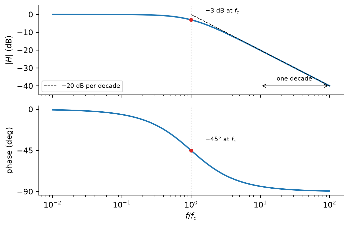
The standard drawing of the third portrait is the Bode plot (Figure 6.2): magnitude in decibels and phase in degrees, both against frequency on a logarithmic axis. Two words of the trade go with it. A decade is a factor of ten in frequency (10 Hz to 100 Hz, 100 Hz to 1 kHz); on the logarithmic axis every decade is the same width. And Lecture 3’s rule that each factor of ten in amplitude is 20 dB means that a response falling as \(1/f\) — the RC filter above its cutoff — drops by 20 dB per decade, which appears on the Bode plot as a straight line of that slope. An ideal amplifier’s Bode plot is the dullest possible: a flat line at \(20\log_{10}G\) and zero phase, which is what “frequency-independent gain” means.
Figure 6.2: The Bode plot of Lecture 3’s RC low-pass filter: magnitude in dB (top) and phase in degrees (bottom) against frequency normalized to the cutoff, on a logarithmic axis. Above the cutoff the magnitude falls 20 dB per decade (the dashed asymptote) and the phase heads toward a 90° lag; at the cutoff itself the response is −3 dB and −45°.
How one gets from portrait 1 to portrait 3 is a calculation you will not need to perform in this course, but you should know its name, because every filter design handbook speaks it. The Laplace transform turns differentiation into multiplication by a complex variable \(s\), so the RC differential equation becomes the algebraic transfer function\(H(s) = 1/(1 + sRC)\); setting \(s = j2\pi f\) recovers the frequency response of Lecture 3, and the value of \(s\) at which the denominator vanishes — here \(s = -1/RC\) — is called a pole. Every pole adds one more factor of \(1/f\) at high frequency, i.e. another 20 dB per decade of roll-off, which is why filters are counted in poles. Digital filters, which operate on sampled data rather than continuous signals, obey difference equations instead of differential ones, and the z-transform plays the same role for them. Lecture 6 develops the frequency response properly; for the transforms themselves, Oppenheim and Willsky’s chapters on the Laplace and z-transforms (Oppenheim et al. 1997) and the Wikipedia articles on the Laplace transform, z-transform, and Bode plot are good places to start on your own.
6.2.2 Amplification
Lecture 3’s Wheatstone bridge delivers a few millivolts, while the ESP32’s ADC spreads its 12 bits over roughly 3 V — digitized directly, the entire signal would occupy a handful of quantization steps. Amplification scales the signal to fill the converter’s range, ideally as a pure frequency-independent gain (the simplest LTI block there is), realized with the op-amp whose internals we settle in the final section of this lecture.
The numbers make the case without further argument. Lecture 3 found that a 120 Ω gauge with a gauge factor of 2 at 1000 µε, in a quarter bridge on 5 V, yields about 2.5 mV. Lecture 4’s 12-bit, 3.3 V converter has a resolution of \(Q = 3.3/4096 \approx 0.81\) mV (Equation 5.6). Fed directly, the whole 0–1000 µε range spans about three codes — roughly 320 µε per count, which is not a strain measurement so much as a strain rumor. A gain of 100 turns 2.5 mV into 250 mV and three codes into about 310, or 3.2 µε per count; a gain of 1000 fills most of the range with about 3100 codes, 0.32 µε per count. The amplifier has not created information — it has matched the signal’s amplitude to the converter’s grid so that the information the sensor produced survives quantization, exactly the remedy Lecture 4 promised when it observed that quantization error is relative to the reading.
Two cautions belong here. A gain amplifies everything at its input — the signal, the noise the cable picked up, and any offset the bridge had when it was supposed to read zero — so amplification is usually paired with the other three jobs rather than used alone. And “frequency-independent” is an idealization: every real amplifier has a bandwidth beyond which its gain falls, so a gain block is also, quietly, a low-pass filter, a fact that the anti-aliasing section will turn from nuisance into tool.
6.2.3 Level Shifting
A vibration signal swings symmetrically about zero, but a single-supply ADC accepts only voltages between zero and its reference — half of every oscillation would simply be clipped away. Level shifting adds a controlled DC offset that re-centers the signal inside the converter’s window, a gain-plus-offset stage built from the same circuit blocks (the ADXL335 does this internally, which is why it rests near mid-supply at 0 g).
In symbols, the complete scaling stage is affine rather than merely proportional,
\[
v_{out} = G\, v_{in} + V_{off},
\tag{6.1}\]
and the design is two constraints in two unknowns: choose \(G\) so the signal’s peak-to-peak swing fills most (not all) of the converter’s range, then choose \(V_{off}\) so the swing sits in the middle of it. A piezoelectric sensor producing ±100 mV about zero, headed for a 0–3.3 V converter, wants \(G = 10\) and \(V_{off} = 1.65\) V, landing in 0.65–2.65 V with margin on both sides. Lecture 2’s datasheet reading already showed you the same decision made by a manufacturer: at a 3 V supply the ADXL335 outputs 1.5 V at 0 g and swings ±0.9 V over ±3 g, so its 0.6–2.4 V output sits inside the rails — the two supply voltages, 0 and 3 V here, beyond which no circuit can push its output — by design. The offset is not noise to be removed later; it is a known constant that the DATA third subtracts back out — provided someone recorded it.
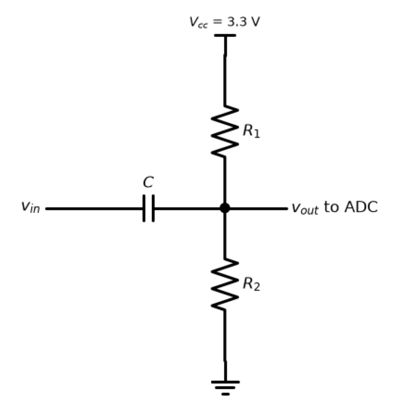
What does a level shifter look like? The simplest one needs no new components at all (Figure 6.3). A capacitor in series passes the changing part of the signal and blocks its DC; on the far side, two equal resistors from the supply to ground hold the node at \(V_{cc}/2\) when nothing is happening, so the signal’s swing now rides on 1.65 V instead of on zero. The price is hidden in Lecture 3: the capacitor and the two resistors (in parallel, as seen from the node) form a high-pass filter with \(f_c = 1/(2\pi (R_1 \| R_2) C)\) — 3.2 Hz for 100 kΩ, 100 kΩ, and 1 µF — so anything slower than that is thrown away along with the DC. For a vibration channel that is a feature; for the ADXL335’s static tilt reading it would be fatal, which is why the manufacturer built the offset in with an amplifier instead. The op-amp version, which adds the offset without blocking anything, appears in the last section of this lecture once its parts are in hand.
Show the code
with schemdraw.Drawing(show=False) as d: d += elm.Line().right().length(0.5).label("$v_{in}$", loc="left") d += elm.Capacitor().right().label("$C$", loc="top") d += (n := elm.Dot()) d.push() d += elm.Resistor().up().label("$R_1$", loc="bottom") d += elm.Vdd().label("$V_{cc}$ = 3.3 V", fontsize=9) d.pop() d.push() d += elm.Resistor().down().label("$R_2$", loc="bottom") d += elm.Ground() d.pop() d += elm.Line().right().length(1.2).label("$v_{out}$ to ADC", loc="right")fig = plt.figure(figsize=(4.2, 3.6)); draw_to(fig.add_axes([0, 0, 1, 1]), d); plt.show()
Figure 6.3: A passive level shifter: the coupling capacitor blocks the input’s DC, and the two equal resistors bias the output node at half the supply. The three parts also form a high-pass filter, so the circuit shifts only signals faster than its cutoff.
6.2.4 Isolation
A sensor bonded to a motor frame or a distant bridge pier can sit at a very different ground potential than the logger, and connecting them directly drives ground-loop currents through the measurement — or, in a fault, puts dangerous voltage on the DAQ. Isolation passes the signal while breaking the galvanic connection (transformers and opto-couplers are the classic implementations), protecting both the electronics and the data.
“Ground” is a name we give to a node, not a property of the universe: two earth connections tens of meters apart are joined by soil and steel of nonzero resistance, and any current flowing through that path — from machinery, from lighting, from a fault — puts a voltage between them. If the sensor references one ground and the logger another, that voltage appears in series with your millivolt signal and, worse, drives a current around the loop formed by the cable and the earth, which the cable’s own resistance turns into yet another spurious voltage (Figliola and Beasley 2019). Isolation cuts the loop. A transformer couples an AC signal magnetically with no wire between primary and secondary; an opto-coupler turns the signal into light and back; an isolation amplifier packages one of these tricks with the gain stage. You have already met the idea in Lecture 2 without the name: the CR3110-3000 current transformer measures the current in a mains conductor with no electrical connection to it at all — the transducer is the isolation, and that is why a current transformer is the safe way to instrument a 240 V feeder while a shunt resistor is not.
6.2.5 Grounded and Floating Sources
Isolation is the heavy remedy; before reaching for it, you have to know what kind of source you are connecting and which of the instrument’s input configurations to use, because most ground trouble is a mismatch between the two. National Instruments’ field-wiring guide, which every data-acquisition vendor’s manual echoes, sorts the world into two kinds of source and three kinds of measurement (National Instruments 2024).
A grounded (ground-referenced) source produces a voltage referenced to the building’s ground: any plug-in instrument that does not deliberately float its output, a sensor whose case is bolted to a grounded structure, or an amplifier powered from the mains. A floating source has no connection to earth at all: a battery-powered device, a thermocouple, a transformer secondary, the output of the isolation amplifier of the previous subsection — its two terminals carry a difference, and neither one is anchored to anything. The distinction matters because two “grounds” in the same building are not at the same potential. NI puts the typical difference between the grounds of two instruments on the same power system at 10 to 200 mV — four to eighty times the 2.5 mV strain signal this lecture keeps returning to — and it is larger when the wiring is poor or a fault is in progress.
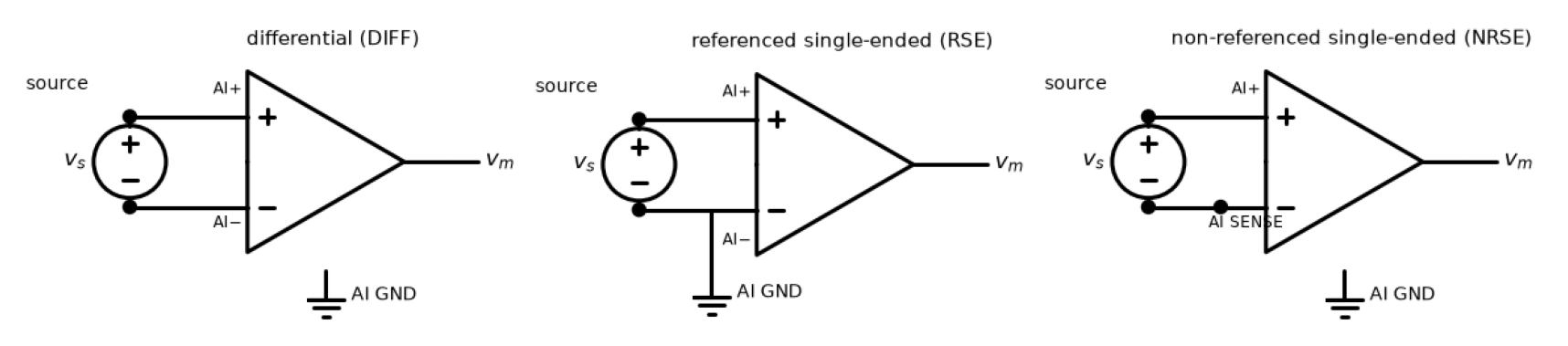
On the instrument side there are three ways to measure a voltage (Figure 6.4), extending the single-ended/differential distinction of Lecture 4 (Section 5.5.1). In a differential (DIFF) measurement, the instrumentation amplifier reads the difference between two input pins, neither of which is tied to the instrument’s ground (AI GND). In a referenced single-ended (RSE) measurement, each input is read against AI GND, which is wired to the instrument’s chassis and to earth. In a non-referenced single-ended (NRSE) measurement, each input is read against a common sense pin (AI SENSE) that all channels share but that is not tied to AI GND — it follows whatever the source’s reference happens to be. Single-ended modes buy twice the channel count of the differential mode, exactly the trade Lecture 4 priced.
Show the code
def config_drawing(mode, title): d = schemdraw.Drawing(show=False) op = elm.Opamp(leads=True).right().flip().at((4, 0)); d += op d += elm.Label().at((op.center[0], op.center[1] +1.6)).label(title, fontsize=10) d += elm.Line().left().at(op.in2).length(1.0) tp = elm.Dot(); d += tp d += elm.Line().left().at(op.in1).length(1.0) bt = elm.Dot(); d += bt d += elm.SourceV().at(bt.center).to(tp.center).label("$v_s$", loc="top") d += elm.Label().at((tp.center[0] -0.9, tp.center[1] +0.35)).label("source", fontsize=9) d += elm.Line().right().at(op.out).length(0.4).label("$v_m$", loc="right") d += elm.Label().at((op.in2[0] +0.25, op.in2[1] +0.3)).label("AI+", fontsize=8)if mode =="RSE": d += elm.Line().down().at(op.in1).length(0.8) d += elm.Ground().label("AI GND", loc="right", fontsize=9) d += elm.Label().at((op.in1[0] +0.25, op.in1[1] -0.3)).label("AI−", fontsize=8)elif mode =="NRSE": d += elm.Dot().at(op.in1) d += elm.Label().at((op.in1[0] +0.25, op.in1[1] -0.3)).label("AI SENSE", fontsize=8) d += elm.Ground().at((op.center[0], op.center[1] -1.5)).label("AI GND", loc="right", fontsize=9)else: d += elm.Label().at((op.in1[0] +0.25, op.in1[1] -0.3)).label("AI−", fontsize=8) d += elm.Ground().at((op.center[0], op.center[1] -1.5)).label("AI GND", loc="right", fontsize=9)return dfig = plt.figure(figsize=(7.6, 2.6))titles = {"DIFF": "differential (DIFF)", "RSE": "referenced single-ended (RSE)","NRSE": "non-referenced single-ended (NRSE)"}for i, mode inenumerate(("DIFF", "RSE", "NRSE")): draw_to(fig.add_axes([i/3, 0, 1/3, 1]), config_drawing(mode, titles[mode]))plt.show()
Figure 6.4: The three input configurations, each measuring a floating source. Differential: the amplifier reads the difference between two pins, neither tied to the instrument ground. Referenced single-ended: the negative pin is the instrument ground itself. Non-referenced single-ended: the negative pin is a shared sense node that floats with the source’s reference.
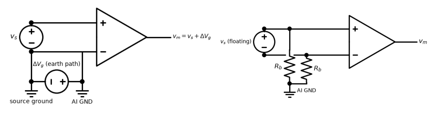
Which configuration fits which source is the whole content of the guide’s first table, reproduced in Table 6.1. A grounded source into an RSE input is the one combination to avoid, and Figure 6.5 (left) shows why: the source’s reference and the instrument’s ground are now joined twice — once by the signal’s return wire and once by the earth between the two grounding points — and the potential difference \(\Delta V_g\) between those two grounds appears in series with the signal. The amplifier reports \(v_m = v_s + \Delta V_g\), and the 10–200 mV of \(\Delta V_g\) simply swallows a millivolt-scale measurement. Worse, the closed loop carries a circulating current that can be large, which is the ground loop named in the previous subsection. Differential and NRSE inputs break the loop by not tying the return to AI GND, and reject \(\Delta V_g\) as a common-mode voltage — the instrumentation amplifier of the last section of this lecture is the part that does the rejecting.
Table 6.1: Input configuration versus source type, after National Instruments (National Instruments 2024).
Source
DIFF
RSE
NRSE
Grounded
recommended
not recommended (ground loop)
recommended
Floating
recommended, with bias resistors
acceptable
recommended, with bias resistors
A floating source has the opposite problem: nothing anchors it. Its terminals could drift to any potential relative to the instrument — and something will push them, because the instrumentation amplifier’s inputs need a tiny bias current to operate, and a floating source offers that current no path to ground. Left unanchored, the source’s common-mode voltage wanders until it leaves the amplifier’s input range, and the reading pins at full scale. The cure is a bias resistor (or two) from the input pins to AI GND (Figure 6.5, right), which gives the bias current a return path while still letting the source float. NI’s guidance is 10 kΩ to 100 kΩ: large enough not to load the source (Lecture 3’s rule — for the 350 Ω bridge, 10 kΩ per side is a 1.7% loading error, 100 kΩ under 0.2%) and small enough that the bias current dropped across it stays well inside the input range. One resistor on the negative input suffices for a low-impedance DC-coupled source such as a thermocouple; use two of equal value when the source is AC-coupled or its impedance is high, so the two inputs stay balanced. RSE needs none, because its negative pin is the instrument ground. The rule to remember: floating source + DIFF or NRSE = bias resistors, or your data will sit at a rail.
Show the code
with schemdraw.Drawing(show=False) as dg: op = elm.Opamp(leads=True).right().flip().at((5, 0)); dg += op dg += elm.Line().left().at(op.in2).length(2.2) tp = elm.Dot(); dg += tp dg += elm.Line().left().at(op.in1).length(2.2) bt = elm.Dot(); dg += bt dg += elm.SourceV().at(bt.center).to(tp.center).label("$v_s$", loc="top") dg += elm.Line().down().at(bt.center).length(1.3) g1 = elm.Dot(); dg += g1 dg += elm.Ground().label("source ground", loc="bottom", fontsize=9) dg += elm.Line().down().at(op.in1).length(1.3) g2 = elm.Dot(); dg += g2 dg += elm.Ground().label("AI GND", loc="bottom", fontsize=9) dg += elm.Line().right().at(g1.center).length(0.5) dg += elm.SourceV().right().length(g2.center[0] - g1.center[0] -1.0).label("$\\Delta V_g$ (earth path)", loc="top", fontsize=9) dg += elm.Line().right().tox(g2.center[0]) dg += elm.Line().right().at(op.out).length(0.4).label("$v_m = v_s + \\Delta V_g$", loc="right", fontsize=9)with schemdraw.Drawing(show=False) as db: op = elm.Opamp(leads=True).right().flip().at((5.4, 0)); db += op db += elm.Line().left().at(op.in2).tox(3.2) t1 = elm.Dot(); db += t1 db += elm.Line().left().tox(2.0) tp = elm.Dot(); db += tp db += elm.Line().left().at(op.in1).tox(4.0) b1 = elm.Dot(); db += b1 db += elm.Line().left().tox(3.4) # gap: the upper bias lead crosses here, no junction db += elm.Line().left().at((3.0, b1.center[1])).tox(2.0) bt = elm.Dot(); db += bt db += elm.SourceV().at(bt.center).to(tp.center).label("$v_s$ (floating)", loc="top", fontsize=9) db += elm.Line().down().at(t1.center).length(1.0) db += elm.Resistor().down().length(1.6).label("$R_b$", loc="top") gb = elm.Dot(); db += gb db += elm.Ground().label("AI GND", loc="right", fontsize=9) db += elm.Resistor().down().at(b1.center).length(1.3).label("$R_b$", loc="bottom") db += elm.Line().down().toy(gb.center) db += elm.Line().left().tox(gb.center) db += elm.Line().right().at(op.out).length(0.4).label("$v_m$", loc="right")fig = plt.figure(figsize=(7.6, 3.0))draw_to(fig.add_axes([0.0, 0, 0.5, 1]), dg); draw_to(fig.add_axes([0.5, 0, 0.5, 1]), db)plt.show()
Figure 6.5: Left: a grounded source read by a referenced single-ended input. The earth between the two grounds closes a loop, and the ground potential difference adds directly to the signal. Right: a floating source read differentially, with two bias resistors to AI GND giving the amplifier’s input bias currents a return path without tying the source to ground.
6.2.6 Filtering
Even a well-scaled, well-centered signal arrives contaminated with content the measurement does not want — 60 Hz hum coupled from power wiring, high-frequency switching noise from nearby electronics. Filters are the frequency-selective LTI circuits that pass the band of interest and attenuate the rest — Lecture 3’s RC low-pass and high-pass are the prototypes — and one low-pass duty in particular, anti-aliasing, matters enough to earn its own section below.
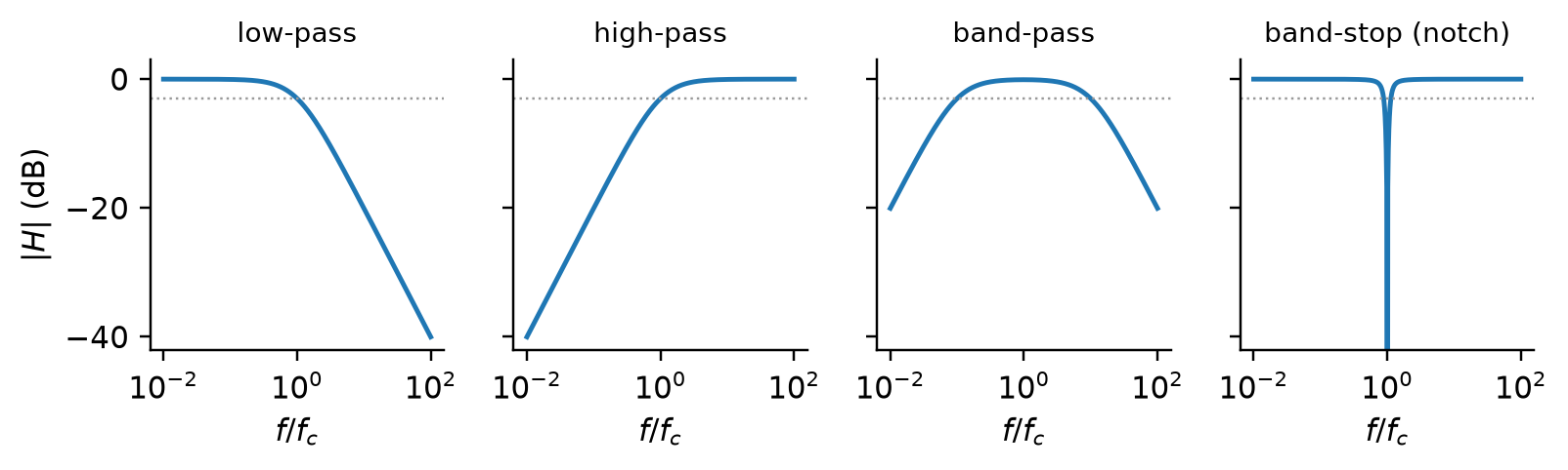
Filters come in various shapes but the common ones are four (Figure 6.6), named for what they let through. A low-pass filter passes frequencies below its cutoff \(f_c\) and attenuates those above — Lecture 3’s RC circuit with the output taken across the capacitor, cutoff \(f_c = 1/(2\pi RC)\) (Equation 4.19). A high-pass filter does the reverse, blocking DC and slow drift while passing changes; the same R and C with the output across the resistor. A band-pass filter is a high-pass followed by a low-pass and keeps only a window of frequencies; a band-stop (or notch) filter removes one — the 60 Hz notch in front of a strain channel is the standard example. Every one of them is characterized by its magnitude response \(|H(f)|\), and two vocabulary items carry the design conversation: the cutoff (where \(|H|\) has fallen to \(1/\sqrt{2}\), i.e. −3 dB) and the roll-off, how fast \(|H|\) falls beyond it. A first-order filter — one R and one C, one pole in the language of Section 6.2.1 — rolls off at 20 dB per decade: a factor of 10 in amplitude for every factor of 10 in frequency. Cascading stages, or wrapping them around an op-amp to make an active filter, steepens the roll-off to 20 dB per decade per pole; Figliola and Beasley’s chapter on analog devices develops the Butterworth family that engineers reach for when one pole is not enough (Figliola and Beasley 2019).
Figure 6.6: The four filter shapes against normalized frequency, with the −3 dB level dotted: a response passes a frequency where it sits above that line. The low- and high-pass curves are first-order (one-pole) responses, exactly Lecture 3’s two RC outputs. The band-pass cascades a first-order high-pass (corner at 0.1) with a first-order low-pass (corner at 10), and the notch is a second-order section centered at 1, where its response falls to zero (−∞ dB) and leaves the plot; both are therefore two-pole responses.
6.3 Sampling
Lecture 4 handed you the sampling theorem and the folding formula as rules to obey, but a rule without a mechanism is hard to trust: why does a 10 Hz tone sampled at 12 Hz masquerade as 2 Hz? Modeling sampling as multiplication of the signal by an impulse train exposes the mechanism — multiplication in the time domain is convolution in the frequency domain (a duality Lecture 6 develops properly), so sampling replicates the signal’s spectrum at every multiple of \(f_s\), and the theorem is exactly the condition that the replicas do not overlap.
Start with the model. An ideal sampler keeps the value of \(y(t)\) at the instants \(t = n\,\delta t\) and discards everything between, which is what you get by multiplying \(y(t)\) by a train of unit impulses spaced \(\delta t\) apart,
The product is zero everywhere except at the sample instants, where it carries exactly the sample values — the stem plot of Lecture 4, written as a function.
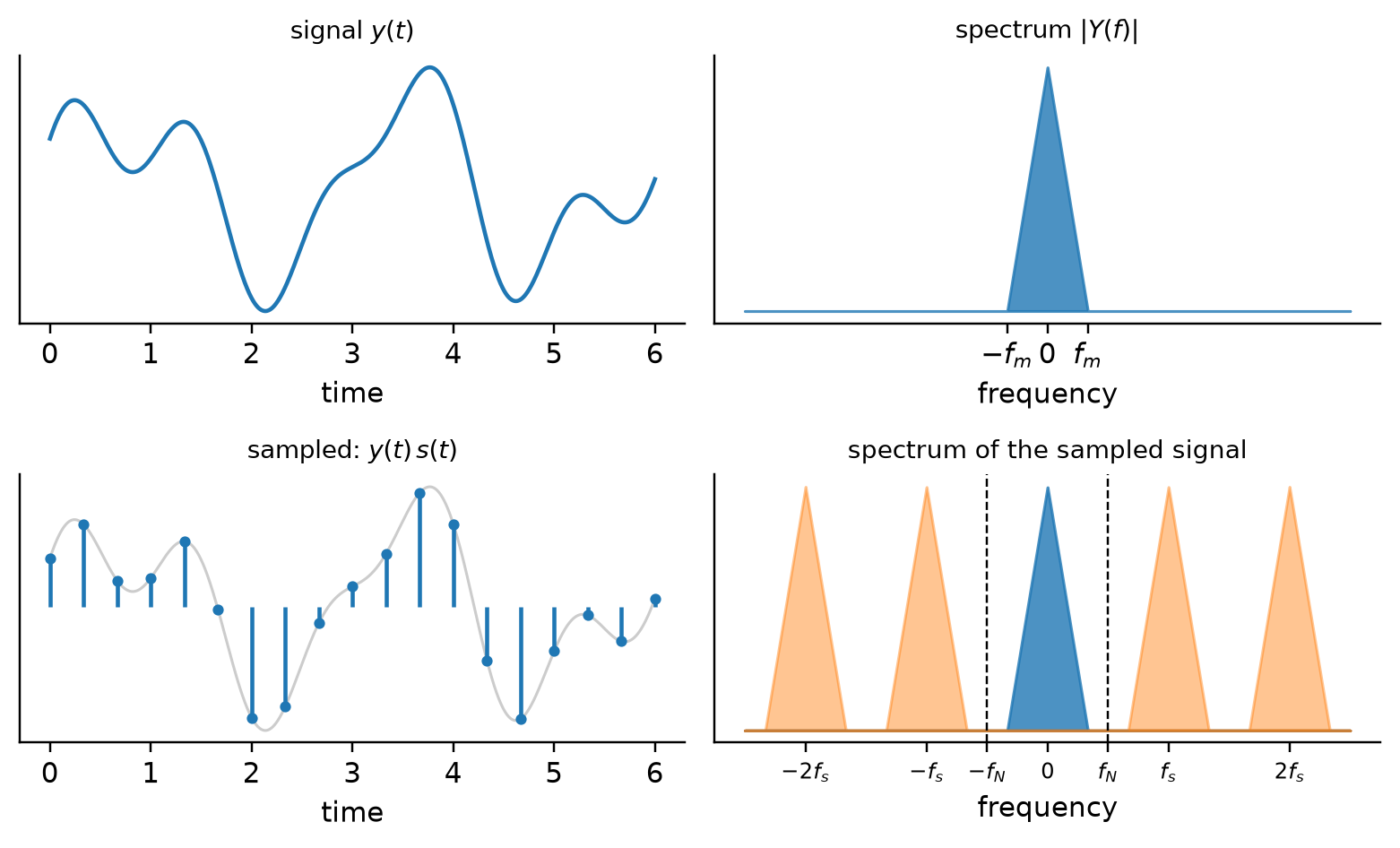
Though we have not yet formally covered the transformation between time-domain signals like the one above and frequency-domain ones — Lecture 6 does — we can keep things simple, because one of the best ways to understand the nature of aliasing is to see the process in Equation 6.2 in the frequency domain. The impulse train is periodic, so (as Lecture 6 will show) its spectrum is also an impulse train, with spikes at every multiple of \(f_s = 1/\delta t\); and because multiplying two signals in time convolves their spectra in frequency, the spectrum of the sampled signal is the spectrum of \(y\) copied onto each of those spikes:
\[
Y_s(f) = f_s \sum_{k=-\infty}^{\infty} Y(f - k f_s).
\tag{6.3}\]
Figure 6.7 draws the four objects side by side. Sampling has not destroyed the original spectrum — there it is, centered on \(k = 0\) — but it has surrounded it with replicas centered on \(\pm f_s, \pm 2 f_s, \ldots\). If \(y\) contains no frequency above \(f_m\) — the maximum frequency present, the number Lecture 4 called the highest frequency with meaningful amplitude — each replica occupies \([k f_s - f_m,\, k f_s + f_m]\), and the replicas stay apart exactly when \(f_m < f_s - f_m\), that is, when \(f_s > 2 f_m\): the sampling theorem of Lecture 4 (Equation 5.2), now with its reason attached. In that case a low-pass filter with cutoff at \(f_N = f_s/2\) can pick the \(k = 0\) copy back out and reconstruct \(y(t)\)exactly from its samples, which is the remarkable half of the theorem that the usual “two samples per period” slogan understates.
Figure 6.7: Sampling in both domains. Top: a band-limited signal and its spectrum, which is zero above \(f_m\). Bottom: multiplying by the impulse train keeps only the sample values (left) and convolves the spectrum with a train of spikes at multiples of \(f_s\) (right), producing replicas that do not overlap because \(f_s > 2 f_m\) here. A low-pass filter at \(f_N\) (dashed) would recover the original spectrum untouched.
One remark keeps later lectures honest. Sampling is not a linear time-invariant operation — slide the input by half a sample period and the output is a different set of numbers, not a shifted copy — so the transfer-function toolkit of Lectures 2 and 3 does not apply to it. That toolkit belongs to the conditioning blocks around the sampler. Sampling has its own algebra, which the next subsection writes out in two lines.
Watch the mechanism directly: the signal is three tones, and the slider sets \(f_s\). As the rate drops, the replicas (orange) slide toward the baseband (shaded) until they land inside it — and each tone that crosses \(f_N\) reappears at the frequency the folding formula predicts.
replicaPlot = {const tones = [{f:3,a:1.0}, {f:7,a:0.6}, {f:11,a:0.4}];const fs = rep.fs, fN = fs /2;const fold = f =>Math.abs(f - fs *Math.round(f / fs));const t = [], samp = [];for (let i =0; i <=800; i++) {const tt = i /800; t.push({t: tt,v: tones.reduce((s, o) => s + o.a*Math.sin(2*Math.PI* o.f* tt),0)}); }for (let k =0; k / fs <=1; k++) samp.push({t: k / fs,v: tones.reduce((s, o) => s + o.a*Math.sin(2*Math.PI* o.f* k / fs),0)});const spec = []; tones.forEach(o => { spec.push({f: o.f,a: o.a,kind:"original"});if (rep.show) for (const k of [-2,-1,1,2]) for (const sgn of [1,-1]) {const fr = k * fs + sgn * o.f;if (fr >0&& fr <=45) spec.push({f: fr,a: o.a,kind:"replica"}); } });const aliased = tones.map(o =>`${o.f} Hz → ${fold(o.f).toFixed(2)} Hz${o.f> fN ?" (aliased)":""}`).join(" · ");returnhtml`<div style="font-family:sans-serif"><b>f_N = ${fN.toFixed(2)} Hz</b> ${aliased}${Plot.plot({width:640,height:200,x: {label:"time (s)"},y: {label:"amplitude"},marks: [Plot.line(t, {x:"t",y:"v",stroke:"#bbb"}), Plot.dot(samp, {x:"t",y:"v",fill:"steelblue",r:3})]})}${Plot.plot({width:640,height:220,x: {label:"frequency (Hz)",domain: [0,45]},y: {label:"amplitude",domain: [0,1.15]},color: {legend:true,domain: ["original","replica"],range: ["steelblue","darkorange"]},marks: [Plot.rect([{x1:0,x2: fN}], {x1:"x1",x2:"x2",y1:0,y2:1.15,fill:"#eee"}), Plot.ruleX([fN], {stroke:"black",strokeDasharray:"4,3"}), Plot.text([{x: fN,y:1.1,l:"f_N"}], {x:"x",y:"y",text:"l",dx:10}), Plot.ruleX(spec, {x:"f",y:"a",stroke:"kind",strokeWidth:2.5}), Plot.dot(spec, {x:"f",y:"a",fill:"kind",r:3})]})}</div>`;}
6.3.1 Aliasing
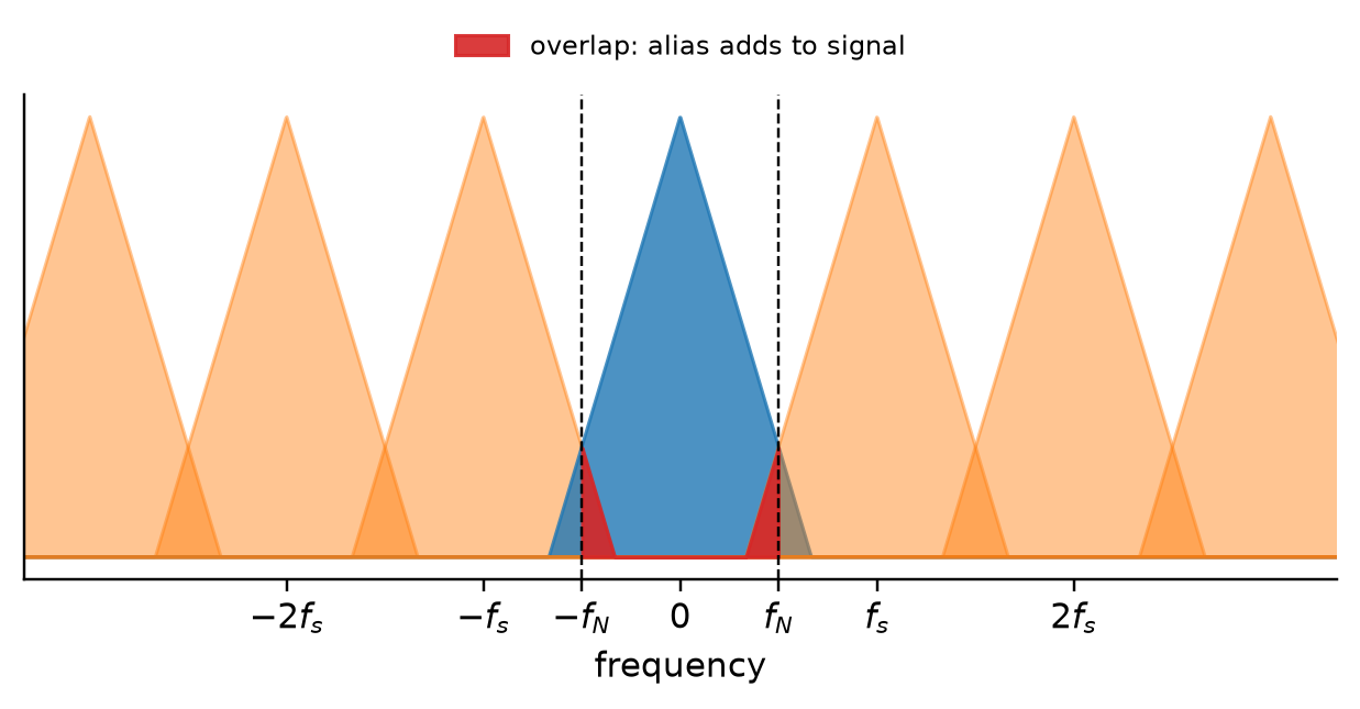
When the replicas do overlap, high-frequency content lands on top of low-frequency content, and nothing downstream can pull the two apart again. Lecture 4’s folding formula, \(f_a = |f - f_s \cdot \mathrm{round}(f/f_s)|\), falls straight out of the replica picture — the alias is simply the distance from \(f\) to the nearest replica center — which is why folding is symmetric about multiples of the Nyquist frequency.
The same conclusion follows from two lines of trigonometry that need no spectra at all, and they are worth seeing because they show that aliasing is an identity, not an approximation (Figliola and Beasley 2019). Sample the tone \(y(t) = C\sin(2\pi f t + \phi)\) at \(t = r\,\delta t\), \(r = 0, 1, \ldots, N-1\), and let \(m\) be any integer. Because \(f_s\,\delta t = 1\), the quantity \(2\pi m f_s r\,\delta t = 2\pi m r\) is a whole number of turns, and a sine does not notice whole turns:
\[
y(r\,\delta t) = C\sin(2\pi f r\,\delta t + \phi) = C\sin\!\big(2\pi (f + m f_s)\, r\,\delta t + \phi\big).
\tag{6.4}\]
Every tone at \(f + m f_s\) produces the very same list of numbers as the tone at \(f\). Run the argument with a minus sign, \(\sin(2\pi m r - \theta) = -\sin\theta\), and the tone at \(m f_s - f\) joins the family too, with its sign flipped — the mirror image that makes folding symmetric about \(f_N\). The sampled record is therefore consistent with an infinite ladder of frequencies \(|m f_s \pm f|\), and the reconstruction filter of Figure 6.7, having no other information, reports the one that lies below \(f_N\): the alias of Equation 5.4. Figure 6.8 shows what the spectrum looks like when this happens to a band of frequencies rather than to a single tone.
Show the code
fs2 =1.5fig, ax = plt.subplots(figsize=(7.0, 2.6))for k inrange(-3, 4): ax.fill_between(ff, tri(ff - k*fs2), color="C0"if k ==0else"C1", alpha=0.8if k ==0else0.45)fb = ff[np.abs(ff) <= fs2/2] # the basebandneighbors = np.maximum(tri(fb - fs2), tri(fb + fs2))ax.fill_between(fb, np.minimum(tri(fb), neighbors), color="C3", alpha=0.9, label="overlap: alias adds to signal")for x in (-fs2/2, fs2/2): ax.axvline(x, color="k", ls="--", lw=0.8)ax.set_xticks([-2*fs2, -fs2, -fs2/2, 0, fs2/2, fs2, 2*fs2])ax.set_xticklabels(["$-2f_s$", "$-f_s$", "$-f_N$", "0", "$f_N$", "$f_s$", "$2f_s$"])ax.set_yticks([]); ax.set_xlabel("frequency"); ax.set_xlim(-5, 5)ax.legend(fontsize=8, loc="lower center", bbox_to_anchor=(0.5, 1.02), frameon=False)plt.show()
Figure 6.8: Aliasing in the replica picture: the same signal as in the previous figure, sampled at \(f_s = 1.5 f_m\) instead of \(3 f_m\). The replicas now overlap the baseband (dark), and whatever lands there adds to the genuine content indistinguishably — no filter applied after this point can separate the two.
Aliasing is not a laboratory curiosity; you have watched it happen. A video camera samples the scene at its frame rate, and a rotor whose blades pass the camera at an exact multiple of that rate produces an alias at \(f_a = 0\): the blades appear frozen in mid-air. A rate slightly off the multiple gives a small alias, and the blades seem to turn slowly, sometimes backwards — the same effect wagon wheels showed in every Western ever filmed.
Video is aliasing you can see. What follows is aliasing you can hear, which turns out to be far more persuasive. The widget below synthesizes one or two pure tones, samples them at a rate you choose, and plays back what an ideal reconstruction filter would recover — the tone itself when it lies below \(f_N\), its alias when it does not. The frequency-domain plot marks both; the time-domain plot shows the samples (dots) that the two candidate tones share.
foldF = (f, fs) =>Math.abs(f - fs *Math.round(f / fs));rcMag = (f, fc) =>1/Math.sqrt(1+ (f / fc) **2);playTones = (tones, dur =1.5) => {const Ctx =window.AudioContext||window.webkitAudioContext;if (!Ctx) return;const ctx =newCtx();const master = ctx.createGain();const total = tones.reduce((s, o) => s +Math.abs(o.a),0) ||1; master.gain.setValueAtTime(0, ctx.currentTime); master.gain.linearRampToValueAtTime(0.25/ total, ctx.currentTime+0.02); master.gain.setValueAtTime(0.25/ total, ctx.currentTime+ dur -0.05); master.gain.linearRampToValueAtTime(0, ctx.currentTime+ dur); master.connect(ctx.destination); tones.forEach(o => {if (o.f<=0||Math.abs(o.a) <1e-6) return;const osc = ctx.createOscillator(); osc.type="sine"; osc.frequency.value= o.f;const g = ctx.createGain(); g.gain.value=Math.abs(o.a); osc.connect(g); g.connect(master); osc.start(); osc.stop(ctx.currentTime+ dur); });setTimeout(() => ctx.close(), (dur +0.3) *1000);};makeWav = (tones, fs, dur) => {// 16-bit mono PCM of the *actual samples* x[n] = sum a_k sin(2 pi f_k n / fs)const N =Math.round(fs * dur), buf =newArrayBuffer(44+2* N), v =newDataView(buf);const str = (o, s) => { for (let i =0; i < s.length; i++) v.setUint8(o + i, s.charCodeAt(i)); };str(0,"RIFF"); v.setUint32(4,36+2* N,true);str(8,"WAVE");str(12,"fmt "); v.setUint32(16,16,true); v.setUint16(20,1,true); v.setUint16(22,1,true); v.setUint32(24, fs,true); v.setUint32(28, fs *2,true); v.setUint16(32,2,true); v.setUint16(34,16,true);str(36,"data"); v.setUint32(40,2* N,true);const total = tones.reduce((s, o) => s +Math.abs(o.a),0) ||1;for (let n =0; n < N; n++) {const x = tones.reduce((s, o) => s + o.a*Math.sin(2*Math.PI* o.f* n / fs),0) / total; v.setInt16(44+2* n,Math.round(Math.max(-1,Math.min(1, x)) *32767),true); }return {url: URL.createObjectURL(newBlob([buf], {type:"audio/wav"})),bytes:44+2* N, N};};
aliasAudio = {const tones = [{f: au.f1,a:1}, {f: au.f2,a:0.7}].filter(o => o.f>0);const fs = au.fs, fN = fs /2;const recon = tones.map(o => ({f:foldF(o.f, fs),a: o.a}));const T =0.005, t = [], samp = [];for (let i =0; i <=600; i++) {const tt = T * i /600; t.push({t: tt *1e3,v: tones.reduce((s, o) => s + o.a*Math.sin(2*Math.PI* o.f* tt),0),s:"original"}); t.push({t: tt *1e3,v: recon.reduce((s, o, j) => s + o.a*Math.sin(2*Math.PI* (tones[j].f- fs *Math.round(tones[j].f/ fs)) * tt),0),s:"reconstructed"}); }for (let k =0; k / fs <= T; k++) samp.push({t: k / fs *1e3,v: tones.reduce((s, o) => s + o.a*Math.sin(2*Math.PI* o.f* k / fs),0)});const spec = tones.map(o => ({f: o.f,a: o.a,kind:"original"})).concat(recon.map(o => ({f: o.f,a: o.a,kind:"reconstructed"})));const report = tones.map((o, j) =>`${o.f} Hz → ${recon[j].f.toFixed(0)} Hz${o.f> fN ?" (aliased)":""}`).join(" · ");const b1 =html`<button>▶ play original</button>`; b1.onclick= () =>playTones(tones);const b2 =html`<button>▶ play sampled at ${fs} Hz</button>`; b2.onclick= () =>playTones(recon);returnhtml`<div style="font-family:sans-serif"><b>f_N = ${fN} Hz</b> ${report}<br>${b1}${b2}${Plot.plot({width:640,height:200,x: {label:"time (ms)"},y: {label:"amplitude"},color: {legend:true,domain: ["original","reconstructed"],range: ["#bbb","darkorange"]},marks: [Plot.line(t, {x:"t",y:"v",stroke:"s",strokeDasharray: d => d.s==="reconstructed"?"4,3":null}), Plot.dot(samp, {x:"t",y:"v",fill:"steelblue",r:3})]})}${Plot.plot({width:640,height:200,x: {label:"frequency (Hz)",domain: [0,6500]},y: {label:"amplitude",domain: [0,1.15]},color: {legend:true,domain: ["original","reconstructed"],range: ["#bbb","darkorange"]},marks: [Plot.rect([{x1:0,x2: fN}], {x1:"x1",x2:"x2",y1:0,y2:1.15,fill:"#eee"}), Plot.ruleX([fN], {stroke:"black",strokeDasharray:"4,3"}), Plot.text([{x: fN,y:1.1,l:"f_N"}], {x:"x",y:"y",text:"l",dx:10}), Plot.ruleX(spec, {x:"f",y:"a",stroke:"kind",strokeWidth:2.5}), Plot.dot(spec, {x:"f",y:"a",fill:"kind",r:3})]})}</div>`;}
With the default settings, a 1000 Hz tone and a 3400 Hz tone sampled at 4000 Hz come back as 1000 Hz and 600 Hz: the upper tone has folded about \(f_N = 2000\) Hz and now sits below the lower one. Nothing in the sampled record marks the 600 Hz component as an impostor.
CautionConcept Check: Can a digital filter tell?
Your accelerometer record, sampled at 100 Hz, shows a clean 2 Hz component. A colleague suggests running a digital filter over the data to check whether it is a genuine 2 Hz mode or an alias of something faster. Will that work?
TipAnswer
No. By Equation 6.4 the samples of a 2 Hz tone and of a 98 Hz (or 102 Hz, or 202 Hz) tone are identical lists of numbers. A digital filter only ever sees that list, so it cannot distinguish alternatives that produce the same list — it will pass or remove the 2 Hz component regardless of where it came from. The only way to know is to have prevented the alternatives from reaching the converter in the first place, which is the next section.
6.4 Anti-Aliasing Filters
The audio demo makes the point brutally: once a tone has folded into band, it sits in the data indistinguishable from a genuine tone, so no algorithm applied after sampling can undo it. The only defense is analog and preventive — a low-pass filter ahead of the ADC — and we design the first-order RC version from Lecture 3: place the cutoff to pass the measurement band while attenuating what approaches \(f_N\), accepting the gentle 20 dB/decade roll-off that one pole buys.
Both words in the phrase carry a design requirement. Analog, because the filter must act on the continuous signal, where a 3400 Hz tone and a 600 Hz tone are still different things; after sampling they are the same list of numbers and the distinction is gone. Before the ADC, because it must stand between the source of the unwanted frequencies and the sampler — placing it anywhere downstream, including in software, is the digital-filter fallacy of the concept check above. The filter’s job statement is then simple to write: pass the band you intend to measure, \(0 \le f \le f_B\), essentially untouched, and attenuate everything above \(f_N = f_s/2\) enough that whatever folds back is smaller than you care about — typically smaller than a quantization step or the noise floor. Two frequencies are now in play, and it pays to keep them apart. The band edge\(f_B\) is the highest frequency you need, a property of your question. The theorem’s \(f_m\) is the highest frequency present at the sampler, a property of the signal, and without a filter it is set by whatever pump, fan, or hum happens to be on the wire. The anti-aliasing filter is what lets you design to \(f_B\): it pushes everything above the band down until the signal the sampler sees is, for practical purposes, band-limited.
6.4.1 Designing the First-Order Filter
Lecture 3’s RC low-pass (Equation 4.19) has magnitude response
which is −3 dB at \(f_c\), about −1 dB at \(f_c/2\), −20 dB at \(10 f_c\), and −40 dB at \(100 f_c\): each decade of frequency (a factor of ten, Section 6.2.1) buys 20 dB, the roll-off of a single pole. The design procedure has four steps, and only the last one involves a choice:
Know your band. The band edge \(f_B\) comes from the physics (Lecture 2’s dynamics) and the question you are asking of the data — a footbridge’s modes below 20 Hz, a pump’s imbalance at its rotation frequency, a temperature that changes over minutes.
Place the cutoff at or somewhat above \(f_B\), accepting the passband droop of Equation 6.5: content at \(f_B = f_c\) is already down 3 dB (29%), so a cutoff at \(2 f_B\) keeps the band within 1 dB.
Compute the attenuation at \(f_N\), and at the frequencies that would fold into your band — anything at \(f_s - f_B\) lands on \(f_B\) after folding.
If it is not enough, you have two knobs and one escape: raise \(f_s\) (each decade of oversampling buys 20 dB, since \(f_N\) moves a decade farther out on the roll-off), add poles (each buys another 20 dB/decade), or — the escape — accept the residual because the source has nothing up there anyway.
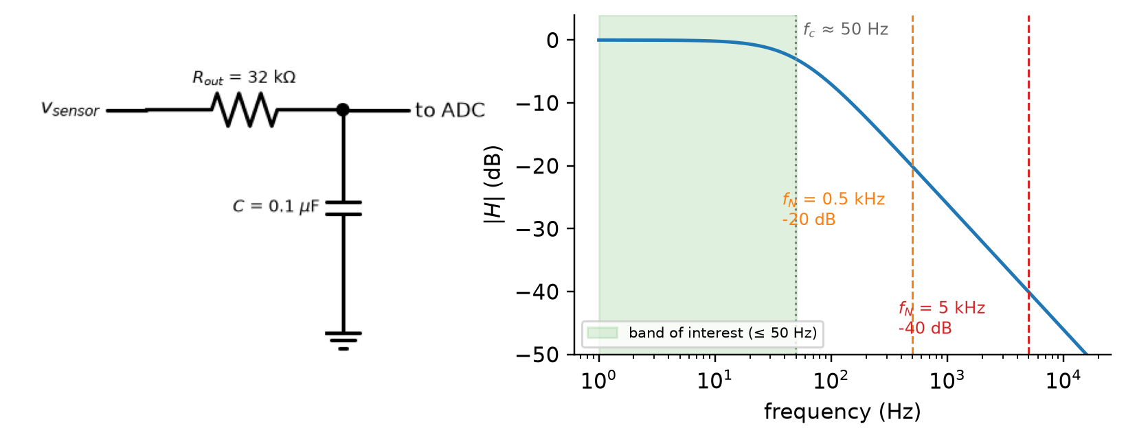
A worked example ties the pieces to hardware you have already met. Take the ADXL335 on the pump housing, logged at \(f_s = 1\) kS/s (\(f_N = 500\) Hz), where the frequencies of interest lie below 50 Hz. Lecture 3’s Exercise 4 already designed this filter without calling it one: the accelerometer’s 32 kΩ output resistance and a 0.1 µF bandwidth capacitor form an RC low-pass with \(f_c = 49.7\) Hz. Its attenuation at \(f_N\) is \(|H(500)| \approx 0.099\), or −20 dB: a 500 Hz disturbance of the same amplitude as the signal arrives at the converter at one-tenth of it. At 950 Hz — the frequency that would alias onto 50 Hz, the top of the band — the attenuation is −25.6 dB. Whether 20 dB is “enough” depends on what you are protecting: it is far short of the 72 dB a 12-bit converter can represent, so a strong 500 Hz component (a motor at 30,000 rpm, say) would still leave a visible alias. Move to \(f_s = 10\) kS/s and \(f_N\) sits at 5 kHz, two decades above \(f_c\), where the same filter delivers −40 dB — oversampling bought 20 dB without touching a component. The datasheet’s bandwidth capacitor is, in other words, the anti-aliasing filter Analog Devices designed on your behalf; your only job is to choose \(C\) with \(f_s\) in mind rather than in isolation.
Figure 6.9: The worked design: the RC anti-aliasing filter formed by the ADXL335’s 32 k\(\Omega\) output resistance and a 0.1 \(\mu\)F capacitor (left), and its magnitude response (right) with the measurement band, the cutoff, and the Nyquist frequencies for two sample rates marked. One pole gives 20 dB at \(f_N = 500\) Hz and 40 dB at \(f_N = 5\) kHz.
A cautionary example closer to home: the GL5528 channel of Assignment 1 has no anti-aliasing filter at all, and it is sampled at 4 S/s, so \(f_N = 2\) Hz. A fluorescent or cheap LED lamp flickers at 120 Hz, which is exactly 30 times the sample rate — its alias is \(f_a = 0\) Hz. The flicker does not appear in your data as a wiggle; it appears as a bias in the mean light level that depends on the phase at which each sample happened to catch the flicker cycle. A dimmed LED driven at some other frequency would alias to a slow, meaningless drift instead. Neither can be diagnosed from the record, which is the whole point of this section.
Hear the difference between the two places a filter can go. The widget adds a first-order RC low-pass to the audio demo, either before the sampler (analog, where it belongs) or after it (digital, on the sampled record). Set tone 2 above \(f_N\) and compare.
With the defaults (3400 Hz tone, \(f_s = 4000\) Hz, \(f_c = 1200\) Hz), the analog filter attenuates the 3400 Hz tone by about 9.6 dB before it can fold, so its 600 Hz alias arrives at a third of its amplitude; move the cutoff down and it fades further. The digital filter, applied to the sampled record, sees the alias already sitting at 600 Hz — comfortably inside the passband — and leaves it essentially untouched. Same filter, same cutoff; only its position in the chain differs, and only one position works.
ImportantExercise: Filter a strain channel
A quarter-bridge strain channel on a footbridge is amplified and then logged at \(f_s = 200\) S/s. The modes of interest lie below 10 Hz. Design a first-order RC anti-aliasing filter using standard components, state its attenuation at \(f_N\) and at the frequency that would fold onto 10 Hz, and say whether the 60 Hz hum a long cable picks up is handled by this filter or needs something else.
TipSolution
\(f_N = 100\) Hz. Place \(f_c\) at about \(2 f_B = 20\) Hz so the band edge loses only about 1 dB: with \(C = 1\) µF, \(R = 1/(2\pi \cdot 20 \cdot 10^{-6}) \approx 7.96\) kΩ — fit the standard 8.2 kΩ, giving \(f_c = 19.4\) Hz. Attenuation at \(f_N = 100\) Hz: \(f/f_c = 5.15\), so \(|H| = 1/\sqrt{1 + 26.5} = 0.191\), about −14.4 dB. The frequency that folds onto 10 Hz is \(200 - 10 = 190\) Hz: \(f/f_c = 9.8\), \(|H| \approx 0.102\), about −19.9 dB. The 60 Hz hum lies below\(f_N\), so it is not an aliasing problem at all — it is sampled faithfully and appears in the record at 60 Hz, attenuated only 10 dB by this filter. Removing it is a job for a notch filter (or a differential input, Lecture 4’s common-mode rejection, which prevents the pickup in the first place).
6.5 Operational Amplifiers
We have now borrowed the op-amp on credit three times — Lecture 4’s follower and comparator, and this lecture’s amplification stage — without asking how a triangle with two inputs does any of it. The answer is negative feedback wrapped around an enormous gain, and two “ideal op-amp” assumptions — no current into the inputs, and equal voltage at the inputs whenever feedback is present — reduce every configuration to an exercise in Lecture 3’s KCL.
6.5.1 The Ideal Op-Amp Rules
An amplifier with a gain of \(10^5\) or more looks useless at first: any honest input slams the output into a supply rail. Negative feedback tames it, and in the feedback regime the two golden rules (zero input current, zero differential input voltage) predict the closed-loop behavior without knowing anything else about the device.
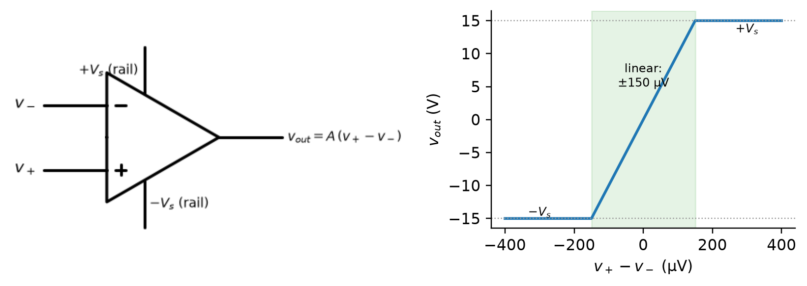
Start with the device itself (Figure 6.10). An operational amplifier is a differential amplifier with two inputs, labeled \(+\) (non-inverting) and \(-\) (inverting), one output, and an open-loop relation
\[
v_{out} = A\,(v_+ - v_-),
\tag{6.6}\]
with \(A\) — the open-loop gain — of order \(10^5\) to \(10^6\) in ordinary parts (Figliola and Beasley 2019). It is powered from two supply voltages, the rails\(\pm V_s\), and its output cannot go past them, so with \(A = 10^5\) and \(\pm 15\) V rails the relation holds only while \(|v_+ - v_-| < 150\) µV; any larger difference parks the output at a rail. Used that way, the op-amp is Lecture 4’s comparator: a one-bit answer to “which input is larger?”
Figure 6.10: The op-amp by itself. Left: the symbol, with its two inputs, its output, and the two supply rails. Right: the open-loop transfer curve for a gain of 100,000 with 15 V rails — a line so steep that the linear region is only 300 µV wide; outside it the output saturates at a rail. Without feedback the device is a comparator.
Negative feedback. Now do something that looks perverse: take a fraction \(\beta\) of the output and feed it back into the inverting input, so that \(v_- = \beta\, v_{out}\) while the signal drives \(v_+ = v_{in}\). Substituting into Equation 6.6 and solving for the output,
The enormous, poorly controlled \(A\) has dropped out, and the closed-loop gain is set by \(\beta\) alone — a quantity you will build from two resistors in the next subsection. Put numbers in: \(A = 10^5\) and \(\beta = 1/100\) give a gain of \(99.9\), within 0.1% of the ideal 100, and for a 10 mV input the output is 0.999 V while the difference between the two inputs is \(v_{out}/A = 10\) µV. That last number is the point. With feedback in place the op-amp drives its own inputs to equality — not because they are wired together, but because any difference between them is amplified until the fed-back output cancels it — and the residual difference is smaller than anything else in the circuit. Feedback is called negative because the fed-back signal opposes the input; feed it into the \(+\) terminal instead and every disturbance is reinforced rather than cancelled, which is how oscillators are made and amplifiers are not.
Why the inputs draw no current. This second fact has nothing to do with feedback; it is a property of the device. The op-amp’s input terminals lead into transistors whose impedance is enormous — megaohms in old bipolar parts, teraohms in modern ones — and with only microvolts across them, Ohm’s law puts the current at picoamps or less (10 µV across 1 MΩ is 10 pA). Against the milliamps flowing in the surrounding resistors that is zero. Together, the two observations are the rules that make op-amp analysis an exercise in Lecture 3’s KCL:
NoteThe ideal op-amp rules
No current flows into either input (a property of the device).
With negative feedback, the output does whatever is necessary to make \(v_+ = v_-\) (a consequence of feedback and the huge open-loop gain).
Rule 2 is often called the virtual short: the two inputs behave as if connected — same voltage — while rule 1 says no current flows between them, so they are not connected. The follower of Lecture 4 is the rules in their simplest form, with \(\beta = 1\): connect the output directly to \(v_-\) and the signal to \(v_+\); rule 2 gives \(v_{out} = v_- = v_+ = v_{in}\), and rule 1 says the source supplies no current — the loading medicine of Lecture 3 in one component.
6.5.2 Inverting and Non-Inverting Amplifiers
The first payoff of the rules is a gain set not by the temperamental op-amp but by two resistors you choose. KCL at the virtual-ground node gives the inverting gain \(-R_f/R_{in}\); moving the signal to the non-inverting pin gives \(1 + R_f/R_g\), with Lecture 4’s unity-gain follower as the special case.
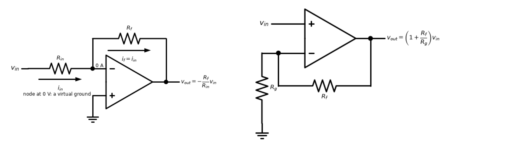
In the inverting amplifier (Figure 6.11, left, with the currents marked) the signal enters through \(R_{in}\), the feedback comes back through \(R_f\), and the \(+\) input is grounded. Four steps, each one rule or one law from Lecture 3:
The \(+\) input is at 0 V, so rule 2 pins the \(-\) input at 0 V as well. That node sits at ground potential without being wired to ground — it is held there by feedback — and is called a virtual ground.
Ohm’s law across \(R_{in}\), from \(v_{in}\) down to the 0 V node: \(i_{in} = v_{in}/R_{in}\).
Rule 1: none of that current can enter the op-amp. KCL at the node then leaves it exactly one way out, through \(R_f\): \(i_f = i_{in}\).
Ohm’s law across \(R_f\), from the 0 V node to the output: \(v_{out} = 0 - i_f R_f\), hence
The gain is a resistor ratio, negative because the output must swing the opposite way to pull current through \(R_f\); with \(R_f = 100\) kΩ and \(R_{in} = 10\) kΩ the gain is −10. Notice what the source sees: the input resistor to a node at 0 V — an input impedance of exactly \(R_{in}\), which loads the source in the sense of Lecture 3’s Equation 4.22.
One more resistor turns this stage into the level shifter promised in Section 6.2.3. Add a second input resistor \(R_2\) from a reference voltage \(V_{ref}\) to the same virtual-ground node, and step 3’s KCL gains one term — two currents arrive, both must leave through \(R_f\) — so
a gain and an offset in one stage, with no capacitor and therefore no lost DC (the sign flip is undone by a second inverting stage, or by choosing \(V_{ref}\) negative). This summing amplifier is the op-amp answer to the level-shifting problem, and the kind of circuit that centers the ADXL335’s output at mid-supply.
In the non-inverting amplifier (right) the signal drives \(v_+\) directly. Rule 2 makes \(v_- = v_{in}\); that node is the midpoint of the divider \(R_f\)–\(R_g\) between \(v_{out}\) and ground, and rule 1 says the divider is unloaded, so \(v_{in} = v_{out}\,R_g/(R_f + R_g)\) and
The divider is precisely the feedback fraction \(\beta = R_g/(R_f + R_g)\) of Equation 6.7, so this is that equation with \(A \to \infty\). The gain is positive, never less than 1 (set \(R_f = 0\) and you have the follower), and the source drives an op-amp input directly — essentially infinite input impedance, no loading. For a gain of 100, \(R_g = 1\) kΩ and \(R_f = 99\) kΩ do it exactly; the off-the-shelf 100 kΩ gives 101, a 1% error that the DATA third would call a calibration constant. This is the configuration for amplifying a sensor whose Thévenin resistance is not negligible — which, after Lecture 3, you know to be most of them.
Figure 6.11: The two workhorse configurations. Left, inverting: the \(-\) input is a virtual ground, no current enters the op-amp, so the input current is forced through \(R_f\) and the gain is \(-R_f/R_{in}\). Right, non-inverting: the feedback divider makes \(v_- = v_{in}\) and the gain is \(1 + R_f/R_g\); with \(R_f = 0\) it is the unity-gain follower.
6.5.3 Difference and Instrumentation Amplifiers
The Wheatstone bridge hands you the difference of two midpoints riding a large common voltage — exactly what Lecture 4’s differential inputs existed for — and a single-op-amp difference stage computes it, but its resistor network loads the bridge. The instrumentation amplifier fixes both problems at once: buffered high-impedance inputs, gain set by a single resistor, and strong common-mode rejection, which is why it is the standard front end for bridge-based sensing.
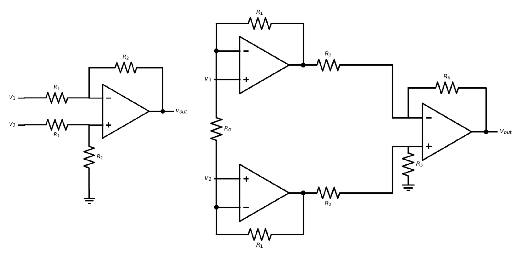
The difference amplifier (Figure 6.12, left) applies both rules at once. The \(+\) input sits at the divider voltage \(v_2\,R_2/(R_1 + R_2)\); rule 2 puts the \(-\) input at the same voltage; and KCL at the \(-\) node with rule 1 gives \((v_1 - v_-)/R_1 = (v_- - v_{out})/R_2\). Eliminating \(v_-\),
provided the two \(R_1\)’s and the two \(R_2\)’s are matched. Any voltage common to both inputs — the 2.5 V that both midpoints of a 5 V quarter bridge sit at — cancels in the subtraction; only the difference is amplified. That is the common-mode rejection that Lecture 4 promised differential inputs would deliver, now built from parts. The catch is loading: the \(v_1\) input sees \(R_1\) to a node held near \(v_2\)’s divided voltage, and the \(v_2\) input sees \(R_1 + R_2\) to ground — finite, and unequal. Lecture 3’s Exercise 5 already priced this: a 350 Ω bridge read through 10 kΩ under-reads by 3.4%, and with the two arms loaded differently the error is not even a clean scale factor. Raising \(R_1\) helps the loading and hurts noise and matching; the tidy fix is different.
The instrumentation amplifier (Figure 6.12, right) puts a non-inverting stage in front of each input, so that each bridge midpoint drives an op-amp input directly — rule 1, no loading at all. The two front-end amplifiers share a single gain resistor \(R_G\) between their inverting inputs: by rule 2 the voltage across \(R_G\) is exactly \(v_2 - v_1\), the current through it is \((v_2 - v_1)/R_G\), and by rule 1 that same current flows through both feedback resistors \(R_1\), so the difference between the two first-stage outputs is \((v_2 - v_1)(1 + 2R_1/R_G)\) while their common-mode component passes through at unity gain. A difference stage then removes the common mode and applies a final ratio:
Integrated instrumentation amplifiers put all three op-amps and the matched resistors on one chip and leave \(R_G\) to you — a single external resistor sets the gain, the inputs load nothing, and the common-mode rejection comes from laser-trimmed matching rather than from your parts bin. For the running bridge: 2.5 mV of difference at 1000 µε riding on 2.5 V of common mode, through an instrumentation amplifier with a gain of 1000, becomes 2.5 V of signal and (ideally) 0 V of common mode — the millivolt that Lecture 3 said had been asking for an amplifier since the middle of the page, delivered to the converter at last.
Figure 6.12: Left, the difference amplifier: matched resistor pairs make the output \((R_2/R_1)(v_2 - v_1)\), but each input is loaded by the resistor network. Right, the three-op-amp instrumentation amplifier: two non-inverting front ends share one gain resistor \(R_G\), so the inputs draw no current and the differential gain \(1 + 2R_1/R_G\) is set by a single part; the output stage is the difference amplifier on the left.
CautionConcept Check: The virtual short
In a working inverting amplifier the two op-amp inputs sit at the same voltage. How much current flows between them, and what would happen to the “same voltage” claim if you removed \(R_f\)?
TipAnswer
None — rule 1. The inputs are at equal voltage not because they are connected but because the output, through \(R_f\), keeps adjusting until they are: a virtual short, enforced by feedback, not a wire. Remove \(R_f\) and the feedback path is gone; rule 2 no longer holds, the tiny input difference is multiplied by the open-loop \(A\), and the output slams into a rail. You have built a comparator.
6.6 Putting It All Together
The measurement chain is now complete — transduction (Lecture 2), circuits (Lecture 3), conversion (Lecture 4), and the conditioning and sampling design of this lecture — and everything the DATA and MODELS thirds do will be done to the output of this chain. One decision distills the whole lecture: choosing \(f_s\) for a given application is a three-way trade between the bandwidth you must capture, the storage and transmission you can afford, and the aliasing risk you are willing to carry — and you will make that trade by ear.
The decision has a definite order of operations, and each step is a section of this course.
Bandwidth first. What is the highest frequency you need to measure, the band edge \(f_B\)? It comes from the physics of the phenomenon and from the sensor’s own dynamics (Lecture 2): a building’s temperature changes over minutes; a footbridge’s modes live below 20 Hz; a pressure transient in a water main lasts milliseconds. Once the anti-aliasing filter has made \(f_B\) the highest frequency present (\(f_m \approx f_B\)), the sampling theorem sets a floor, \(f_s > 2 f_B\), and waveform fidelity suggests 5–10× \(f_B\) if the shape of the signal matters and not only its frequency content.
Aliasing second. What lies above\(f_B\) at the sensor output — machinery, hum, flicker, the sensor’s own resonance — and how much of it will the anti-aliasing filter you can afford remove at \(f_N\)? If one pole at \(f_c \approx 2 f_B\) does not attenuate it enough, the cheapest cure is usually to oversample: every decade of extra \(f_s\) buys 20 dB.
Storage and transmission last, but not least. The data rate is channels × \(f_s\) × bytes per sample, and a month is 2.6 million seconds. Three axes of 16-bit acceleration at 100 S/s is 600 B/s, about 1.6 GB per month; the same at 500 S/s is 7.8 GB. A temperature logged once a minute is 86 kB per month — small enough that no one should ever alias a temperature record to save space. A pressure channel at 1 kS/s is 5.2 GB per month, which is where the wireless node of Lecture 4 starts to care about its radio and its battery, and where the DATA third’s compression lecture earns its place.
The trade is real: a higher \(f_s\) relaxes the filter and captures more, and costs storage, bandwidth, and power in direct proportion; a lower \(f_s\) saves all three and demands a sharper filter and a firmer knowledge of \(f_B\) and of what lies above it. What it is not is a place to economize blindly — Lecture 4’s cautionary tale of the 7 Hz bridge mode logged at 5 S/s is a storage saving of exactly the kind this section exists to prevent.
TipActive Learning: Choose a rate by ear
The widget below plays a signal with components at 440, 880, 1320, and 2640 Hz — a fundamental and three overtones — and lets you choose \(f_s\). Find the lowest sample rate at which the reconstructed signal still sounds like the original, then download the sampled record as a WAV file and check its size. Defend your choice: what is \(f_m\), what does the theorem demand, what did your ear demand, and what would a 30-day recording cost at your rate versus at 48 kHz? Then set \(f_s\) just below your threshold and identify, from the folding formula, the frequency of the intruder you hear.
From here on the signal is a list of numbers, correctly scaled, centered, protected from the frequencies it cannot represent, and sampled at a rate someone chose on purpose. Lecture 6 gives the frequency-domain view its full mathematical form — the transform that turned multiplication into convolution in this lecture — and Lecture 7 asks how much to trust each of those numbers. After that, the DATA third takes custody.
6.7 Exercises
Predict the aliased frequency in each case, and state whether the record can reveal that aliasing occurred:
60 Hz lies above\(f_N = 50\) Hz; nearest multiple of 100 is 100, \(f_a = 40\) Hz.
nearest multiple of 100 to 130 is 100, \(f_a = 30\) Hz.
\(120 = 30 \times 4\) exactly, \(f_a = 0\): the flicker becomes a DC bias.
In no case can the record reveal it — the alias is, by Equation 6.4, sample-for-sample identical to a genuine tone at \(f_a\).
A pressure transducer channel with content of interest up to 200 Hz is sampled at 2 kS/s.
Choose \(f_c\) for a first-order RC anti-aliasing filter and compute its attenuation at \(f_N\).
The specification asks for at least 40 dB at \(f_N\). Show that one pole cannot meet it at this rate, and find the sample rate at which it could.
How many poles at the same \(f_c\) would meet it at 2 kS/s?
TipSolution
\(f_N = 1\) kHz. With \(f_c = 200\) Hz (accepting −3 dB at the band edge) the attenuation at 1 kHz is \(-10\log_{10}(1 + 25) \approx -14.1\) dB.
One pole reaches −40 dB at \(f/f_c \approx 100\), i.e. \(f_N = 20\) kHz, so \(f_s \approx 40\) kS/s — twenty times the original rate, a steep price in storage for a single capacitor saved.
Each pole contributes the same \(-10\log_{10} 26\), so two poles at 200 Hz give \(-20\log_{10} 26 \approx -28.3\) dB at 1 kHz; three give \(-30\log_{10} 26 \approx -42.4\) dB. A third-order filter meets the specification at 2 kS/s; Figliola and Beasley’s Butterworth designs (Figliola and Beasley 2019) give the component values.
An inverting amplifier has \(R_{in} = 4.7\) kΩ and \(R_f = 47\) kΩ.
Find its gain and its output for a 0.12 V input.
Its input is a sensor with a 2 kΩ Thévenin resistance; by how much does the loading change the effective gain?
Design a non-inverting stage with a gain of 100 for the same sensor and explain why the loading problem disappears.
TipSolution
\(G = -47/4.7 = -10\); \(v_{out} = -1.2\) V.
The virtual ground puts the source’s 2 kΩ in series with \(R_{in}\): the effective input resistor is 6.7 kΩ and the gain becomes \(-47/6.7 \approx -7.0\), a 30% error that depends on a sensor property, not on your design.
\(R_g = 1\) kΩ, \(R_f = 99\) kΩ (or 100 kΩ for a gain of 101). The source now drives the \(+\) input directly; by rule 1 it supplies no current, so its 2 kΩ drops no voltage and the gain is independent of it.
Choose and justify a sample rate for each of the following, and compute the storage for a 30-day deployment at 16 bits per sample:
traffic-induced vibration of a highway overpass, three accelerometer axes, modes of interest below 25 Hz;
indoor air temperature in an office, one channel;
pressure transients (water hammer) in a distribution main, one channel, with wavefronts rising in about 5 ms.
TipSolution sketch
\(f_B = 25\) Hz; once the filter has removed what lies above the band, the theorem demands \(> 50\) S/s, waveform fidelity 125–250 S/s. At 200 S/s: \(3 \times 200 \times 2 = 1200\) B/s, about 3.1 GB per month — with an RC anti-aliasing filter at about 50 Hz giving only about −7 dB at \(f_N = 100\) Hz, so either oversample (1 kS/s: 15.6 GB per month, −20 dB) or use a higher-order filter.
Room temperature has time constants of many minutes; one sample per minute is generous and costs 86 kB per month. Filtering is done by the sensor’s own thermal lag (Lecture 2).
A 5 ms rise implies content to a few hundred hertz; sample at 2–5 kS/s. At 2 kS/s: 4 kB/s, about 10.4 GB per month — the case where you would record only around triggered events rather than continuously.
For each channel in Exercise 4, list which of the four conditioning jobs it needs and why, naming the specific circuit from this lecture you would use.
TipSolution sketch
Amplify with an instrumentation amplifier if the accelerometers are bridge-type or piezoelectric with millivolt outputs (an ADXL335 needs none — it is already scaled and level-shifted internally); level-shift to mid-supply for a single-supply ADC; filter with the RC anti-aliasing design; isolate if the overpass and the logger cabinet have separate earths.
Filtering only, and the sensor supplies it for free; a thermistor divider like Assignment 1’s needs no amplifier.
Amplify (transducers are typically millivolt-per-volt bridges — instrumentation amplifier), level-shift if the transient is bipolar about the static pressure, filter for anti-aliasing, and isolate if the transducer body is bonded to a pipe with its own ground.
6.8 Additional Resources
Falstad circuit simulator — interactive op-amp configurations you can rewire live; the Op-Amps menu has the inverting, non-inverting, and difference amplifiers of this lecture.